<small id="v9s5k"></small><label id="v9s5k"><menuitem id="v9s5k"><font id="v9s5k"></font></menuitem></label>

      Stock Code:002815
      中文

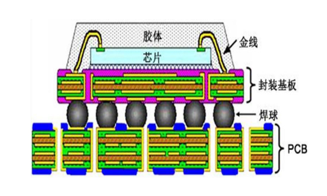
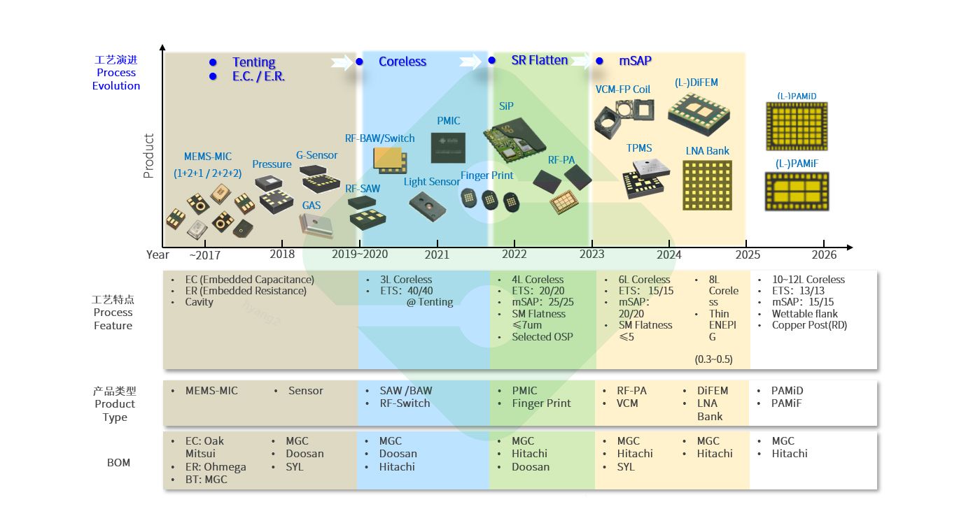
      IC substrates serve as the core component in advanced chip packaging, fulfilling three critical functions: chip protection, electrical interconnection, and thermal management. They surpass conventional PCB capabilities to enable ultra-high-density connectivity between chips and mainboards. Utilizing specialized materials like ABF/BT, they support ultra-fine circuits (line/space to 8μm) and incorporate micro-bumps and redistribution layers for precise I/O connections with sub-micron accuracy. This technology meets rigorous signal and power integrity requirements while enabling advanced architectures like 2.5D/3D integration and chiplets, making it essential for AI, high-performance computing, and premium communication chips.

      • SiPSubstrate

        Craft show

        Layers 2 -8L
        Strip Size 189.0*68.0,70.0*240.0,75.0*240.0, 76.3*240.0, 95.0*240.5etc.
        Unit Size 5.4*6.8,8.1*8.1 / 15*16/ 19*19 etc.
        Material MGC 832NXA / 832NS / 972 Series Hitachi 705G/ 770G Series AUS308 / AUS 320 / SR1
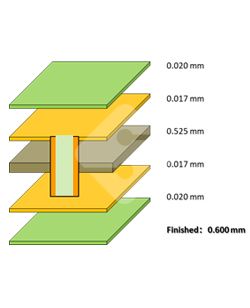
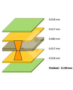
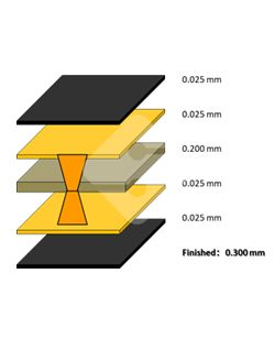
        Finished Thickness 0.120~0.500 mm
        Min. Trace Width/Space 0.025mm / 0.025 mm
        Product Feature Impedance,Selected OSP, SM Coining
        Applications Wearables,Wireless etc.
      • FingerPrintSubstrate

        Craft show

        Layers 2-4L
        Strip Size 75.0*240.0,76.3*240.0etc.
        Unit Size 1.5*4.0 etc
        Material Doosan 7409HGB(LE)/(GQ) Series AUS308
        Finished Thickness 0.500~0.800 mm
        Min. Trace Width/Space 0.040mm / 0.040 mm
        Product Feature SM Coining
        Applications Phone,Wearables,PCetc.
      • Pressure sensor substrate

        Craft show

        Layers 2 ~4 L
        Strip Size 66.0*142.0,50.8*188.95,50.8*152.4, 74.0*240.0,75.0*240.0,76.3*240.0etc.
        Unit Size 2*2/ 3*3 etc.
        Material MGC 832NXA / 832NS Series SYL SI13U / SI10US Series AUS308
        Finished Thickness 0.120~0.500 mm
        Min. Trace Width/Space 0.040mm / 0.040 mm
        Product Feature SM Coining
        Applications Phone,Wearables,PC,Automobileetc.
      • Light Sensor Substrate

        Craft show

        Layers 2 ~4 L
        Strip Size 50.8*188.95,187.5*50.0etc.
        Unit Size 1.5*4.2 etc.
        Material MGC 832NXA / 832NS Series NANYA NPG-180BK / INBK Series AUSMEH / EG23
        Finished Thickness 0.200~0.500 mm
        Min. Trace Width/Space 0.040mm / 0.040 mm
        Product Feature SM Coining
        Applications Phoneetc.
      • Filter Substrate

        Craft show

        Layers 2~4 L
        Strip Size 93.81*93.81,189.0*68.0,75.0*240.0, 100.0*103.0,76.3*240.0etc.
        Unit Size 1814 / 1612 / 1411 / 1109 etc.
        Material MGC 832NS Series Hitachi 705GSeries AUS308 / AUS 320
        Finished Thickness 0.120~0.300 mm
        Min. Trace Width/Space 0.025mm / 0.025 mm
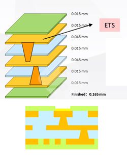
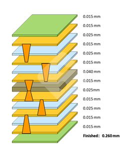
        Product Feature Coreless Structure,ETS Structure
        Applications Phone,Wearablesetc.

      Jiangsu IC Substrate plant

      more

      Follow us

      一级a一级a爰片免费免两_亚洲成av人精品自偷拍_亚洲ⅴa中文字幕无码毛片_亚洲黄无码一区二区三区
      <small id="v9s5k"></small><label id="v9s5k"><menuitem id="v9s5k"><font id="v9s5k"></font></menuitem></label>

          亚洲区小说区激情区图片区 | 亚洲制服类中文字幕 | 六月婷婷国产精品综合 | 午夜欧美精品久久 | 亚洲v欧美v国产v在线成 | 在线网址亚洲精品你懂的 |